Remember: Russia Must Cannibalize for Chips? Think Again
Dated but still very relevant article
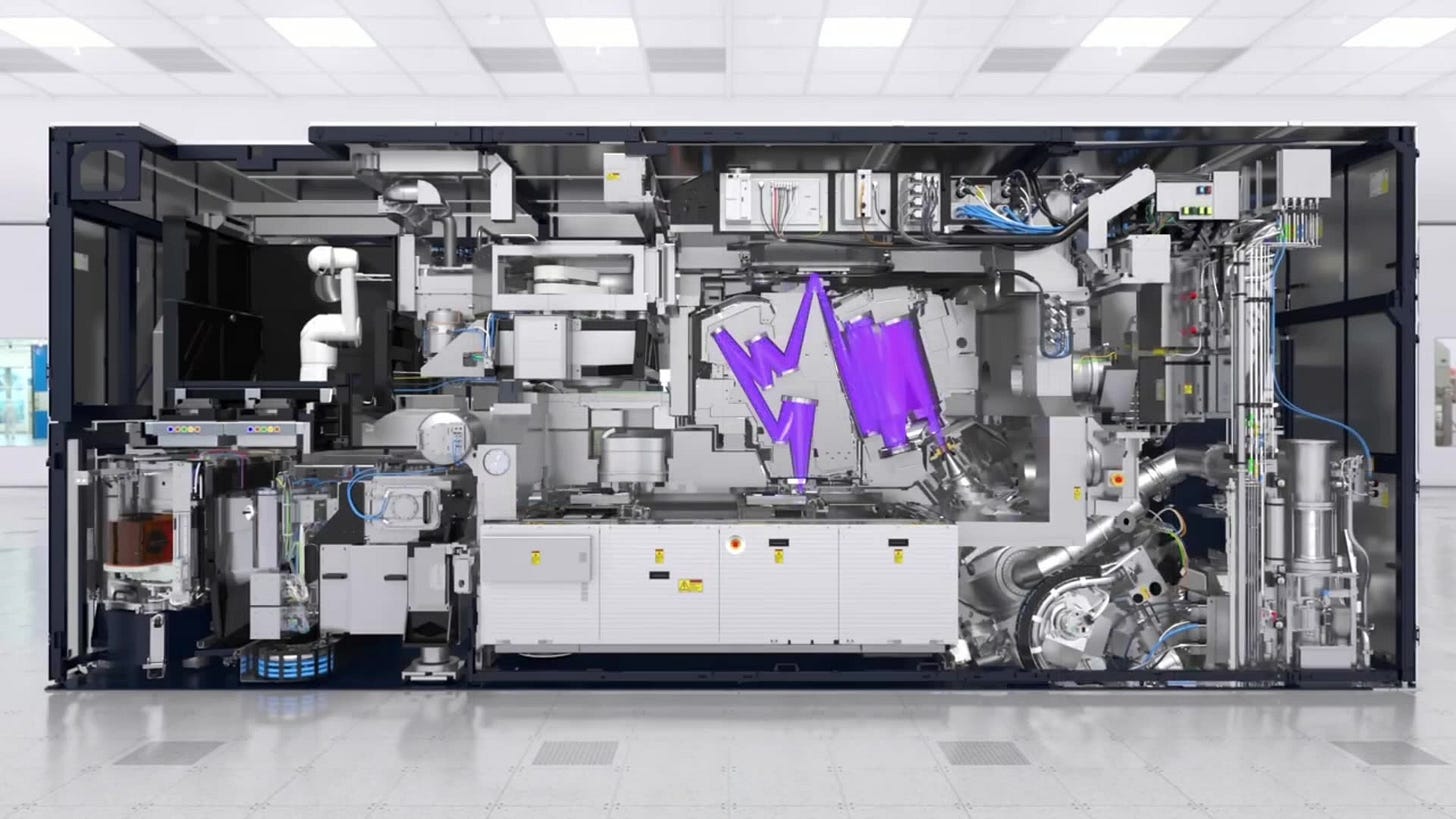
AMSL EUV Machine
Many thanks to the commentator Amrit Nimiyar at Martyanov’s blog for posting the link to the following somewhat dated yet very informative article about the status of state-of-the-art chip making in Russia which was published by/at the Development Strategy of the Nizhny Novgorod Region website on 18 October 2022. Some will recall the massive dissing Russia got from Western BigLie Media because it supposedly had to pirate microprocessors—chips—from dishwashers, washing machines, cars and other consumer products because it couldn’t manufacture its own chips for its weapons. Those of us in-the-know at the time knew that was a BigLie since the Soviet Union made its own chips for its own applications—the sophistication of its missiles, jet aircraft, space rockets, and satellites proved that. But in one respect the charge was correct: Russia was incapable of manufacturing its own lithography machines capable of making current state-of-the-art chips. That became a worrisome problem in 2014 and a very serious problem in 2022 due to the illegal sanctions. Technological sovereignty is something Putin has made a Russian priority during his years of leadership. But as you’ll learn, designing such a machine isn’t at all easy. How does this relate to geopolitics? As with military strength, industrial and scientific prowess is a very major factor determining if a nation is a top, second-, or third-rate power. Simply, Russia’s defense demands it have the top gear technologically.
Nizhny Novgorod may soon surpass the whole world in the production of equipment for the manufacture of microelectronics
Imagine that you need to cut a New Year's snowflake out of paper with garden pruning shears - after all, nail scissors are nowhere to be found. Or draw your eyes with a paint brush, because eyeliner will not be sold to you even for a lot of money.
If you have succeeded, and even more so if you have not been able to imagine it, then you have become one step closer to understanding one of the main difficulties in the production of microelectronics. It turns out to be more productive and energy-efficient, the smaller its computing elements, and for this, the equipment on which it is made must, without exaggeration, be perfect.
Only a few countries now produce truly advanced industrial equipment for microelectronics. But, of course, they are not ready to share everything, not with everyone and not for free.
In fact, the problem of supplying equipment and materials for microelectronics arose much earlier - serious restrictions appeared back in 2010, and even before that, it was only possible to buy equipment that was two or three generations outdated.
But now the Nizhny Novgorod region is ready to take a step - it would seem that only one or two dozen nanometers - should be a technological leap, giving Russia the opportunity to become one of the leading powers in the production of equipment for the manufacture of microelectronic components.
The development became known during the Russian Forum "Microelectronics 2022" - this is the main domestic platform where experts discuss the strategy of scientific and technological development of the industry, present industrial and innovative projects in the field of micro- and radio electronics, and conclude contracts.
We are talking about the key production equipment - the lithograph, which is the most complex and expensive element of any microelectronic production. We can say that lithography is the "heart" of chip production.
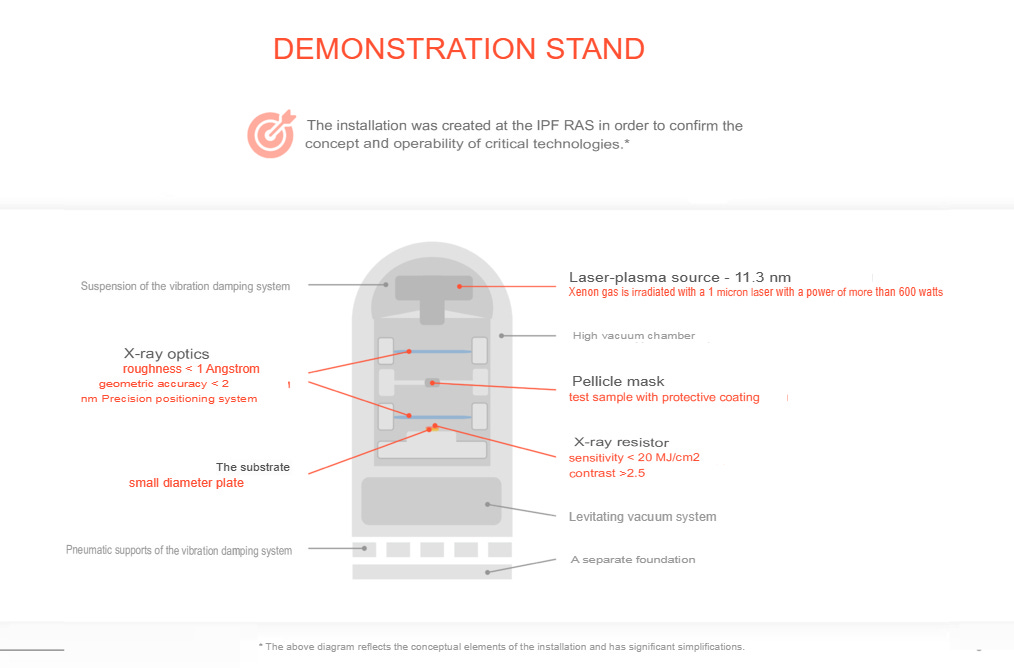
The Nizhny Novgorod delegation presented a demonstration sample of the lithography unit, which was developed, manufactured and installed at the IAP RAS in Nizhny Novgorod. So far, this is not even a prototype of the equipment, but rather a "prototype of a prototype".
The demo version cannot solve real industrial problems, it has another important function - it gives scientists the opportunity to make sure that critical technologies are feasible and test other key hypotheses necessary for further work.
Without this, it would be irrational to start creating a prototype of a lithographic installation, the main goal of Nizhny Novgorod physicists. But in order to understand the importance of this development and its essence, it is necessary to immerse ourselves in an accessible theory for a while.
Small nuances
Not a single country in the world has a full range of technologies and resources necessary for the creation of microelectronics. In part, this is due to the variety of its applications: the space industry requires some solutions, the military-industrial complex needs others, and consumer markets require still others.
And in each of these cases, different materials, equipment are required, and the computing power of the final products may differ by orders of magnitude. All these nuances determine what the so-called "chip" should be.
If we explain using the example of an ordinary computer or smartphone, then the chip is the main internal element of the processor with a size of only a few tens of square millimeters, but at the same time consisting of millions and even billions of transistors that determine the computing capabilities of the future computer.
The production of any chip includes hundreds of technological operations involving dozens of types of equipment and hundreds of different materials. One of the key stages of production is lithography, when a complex and incredibly miniature "pattern" is applied to a silicon base, or in other words, a substrate, and this process is repeated with the same wafer dozens of times, forming a complex "pie".
The process of lithography is a bit like a shadow theater, when there is directional light, an opaque barrier and a canvas on which the resulting image appears. In the same way, a lithograph has a source of radiation, for example, ultraviolet or X-ray, which passes through special optics and a special stencil called a mask, and then its "pattern" is projected onto a substrate.
The substrate itself is pre-coated with light-sensitive compounds — resists — which either protect the substrate from light or, on the contrary, allow it to be "etched", thereby creating volumetric "grooves" on the substrate. After lithography, the resist is removed, numerous operations are performed to deposition various materials, and the lithography process is repeated until a complex architecture of interconnected transistors and other chip elements is formed on the substrate.
But there is also a significant difference from the shadow theater, where the contours of silhouettes are quite clear. Any light (radiation) has a certain wavelength. For example, the human eye sees in the range of 350-750 nanometers, ultraviolet radiation is limited to 100-400 nanometers. And the elements of the chip can be less than a dozen nanometers in size. And when the substrate is irradiated, the resulting picture is blurred like a bad photo. The borders are fuzzy and uneven. This is one of the key problems in the creation of chips.
The leaders of the consumer microelectronics industry have come close to 7 nm - 200 thousand times less than a millimeter. This is close to the theoretical limit - a further reduction - to 1-2 nm - is no longer a real reduction in the size of elements that are in the same plane, but the creation of a "layer cake" - transistors can only be placed one above the other.
The lag of our country in this direction is understandable - in Russia, equipment for lithography was not produced at all before. Even in the days of the USSR, it was made on the territory of Belarus.
Despite the fact that a significant part of microelectronics, including automotive, space, and industrial electronics, is produced at 360-65 nm standards, that is, this lag will not cause critical consequences in the near future, in the long term it will create more and more restrictions for domestic instrumentation, the development of industry and science.
Demo version
Having understood the main points, we can return to the development presented to the forum participants.
Nizhny Novgorod physicists, engineers and designers opted for an X-ray radiation source. It has advantages over the more common photolithography that uses ultraviolet light. Especially when it comes to working with ultra-small areas of the order of 14 nm and less.
There are, however, additional difficulties with it. For example, X-ray radiation requires fundamentally different, perfect optics. The surface of its elements must be smooth down to the atom. It is no exaggeration to say that the permissible roughness cannot exceed 1 Angstrom, which is one ten-millionth of a millimeter.
Another difficulty is the radiation source itself. It must be both powerful and very "accurate": it must emit exactly the wavelength that is needed for operation – up to hundredths of a nanometer. In addition, the radiation source should not contaminate the area where the work processes are taking place.
These critical tasks had to be solved at the stage of creating the demonstrator. And here the domestic developers took their own unique path.
Compared, for example, with the lithographs of the world's leading manufacturer from the Netherlands – ASML, in the Nizhny Novgorod model, the radiation source is many times more compact and cleaner in operation, which ultimately significantly affects the cost, size and complexity of the equipment. The optical system of the demonstrator, produced at IPM RAS, generally surpasses all analogues existing in the world today.
As a result, scientists expect that with the same power of the radiation source, the Nizhny Novgorod installation - no longer demo, but fully operational - will be 1.5-2 times more efficient than the Dutch one.
And there are grounds for such predictions: thanks to the demonstrator alone, individual images on substrates with a resolution of up to the limit of 7 nm were obtained.
In comparison with analogues of the world's leading manufacturers, the Nizhny Novgorod lithograph will:
Cheaper to produce
Leaner
1.5-2 times
more efficient
have a unique
optical system
Three steps from the future
An industrial prototype of the lithograph is planned to be created in six years. Earlier, as in the case of any other high-tech developments, it is necessary to overcome several stages, gradually introducing elements of automation, increasing the power of the source, and complicating the optical scheme.
Step One
By 2024, an alpha machine should be developed. In fact, from this moment on, the installation will become working equipment and will be designed to carry out a full cycle of operations. However, the emphasis at this stage will not be on the high speed of its operation or resolution, but on the full implementation of all systems.
However, this should be enough to make the development attractive to investors and factories, especially given the competitive cost of the plant itself and its maintenance.
Step two
By 2026, alpha should be replaced by beta. All systems will be improved and complicated, resolution will increase, productivity will increase, and many operations will be robotized. The unit can already be used in large-scale production, which will be done — at this point, it is important to integrate it into real technological processes and debug it by "pulling up" the appropriate equipment for other stages of production.
Step Three
At the final stage of development, the lithograph will acquire a more powerful radiation source, improved positioning and feeding systems, and will work quickly and accurately. This should happen as early as 2028.
The birth of Russia's own production of an ultra-precise modern lithograph is not a local achievement, but without exaggeration, an event on a planetary scale. Many countries of the world, for example, China, are literally hunting for such technologies, and simply for the purchase of such equipment. So the domestic development will definitely not remain without demand.
Moreover, after its industrial implementation, it will be possible to talk with all reason about not just abstract leading positions in the field of creating equipment for the production of the most important elements of microelectronics. This is an approach to the full technological sovereignty of Russia and, as a result, the exclusion of many significant risks to national security and the economy. [All Emphasis Original]
Yes, the goal is the export market as well as satisfying domestic demand. Russia has proven that you don’t need the best chips to make the best aircraft, missiles and rockets. Imagine what it might produce having them. IMO, by mid-century if not earlier, Eurasian nations will be the leaders in electronics, computing, and other related technical fields and will be leaders of that vast market.
*
*
*
Like what you’ve been reading at Karlof1’s Substack? Then please consider subscribing and choosing to make a monthly/yearly pledge to enable my efforts in this challenging realm. Thank You!
.


As of 5 or 6 years ago [before I retired], both the Russians and Chinese were ahead of the US and EU in applying Gallium Nitride (GaN), over Gallium Arsenide semiconductors in transportable and airborne radar applications and the result is longer intercept ranges over US/EU systems. It was a little reported technology gap.
GaN better heat resistance allowed higher energy power supplies for radar and radio transmitter chains. The heat tolerance allows more power which means more range for the RF emissions.
Russia and China must be "printing" some advanced microcircuits at least in power supply applications.
US is catching up, the SPY 6 (New Aegis) has some GaN and a new radar for F-35 (which adds to its power/heat containment issues) should use GaN.
I can't imagine PRC has not got a lot of data on those Dutch printers TSMC uses!!
good for russia! screw these sanction crazy control freaks who want to dominate and bully others via financial or other types of sanctions.. go russia!!